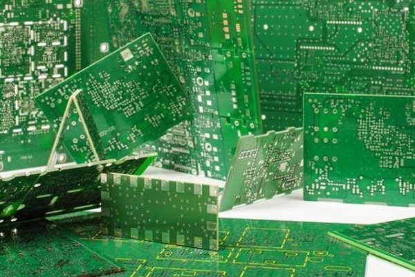
If you open any electronic device, you will most likely come across a PCB or printed circuit board because it is one of the most widely used parts in electricity and electronics. On this board, the installation of electronic components and the design of connections between them have been done. Printed circuit boards, with more than half a century of common use in the electronics industry, have now become complex products that are designed and produced by experienced designers and following precise processes. Although it is not necessary for designers to know how to make PCBs, people who know about these processes are better able to design a low-cost printed circuit board, and in this way, they can get more profit from its production. In this section of the Arya Madar Arjomand website, we intend to provide you with useful information regarding the types of final coating of printed circuit boards or single-sided and double-sided PCBs and their constituent layers.

In the following, we would like to provide tips about the types of final cover of the printed circuit board.
Single-sided PCB printed circuit boards
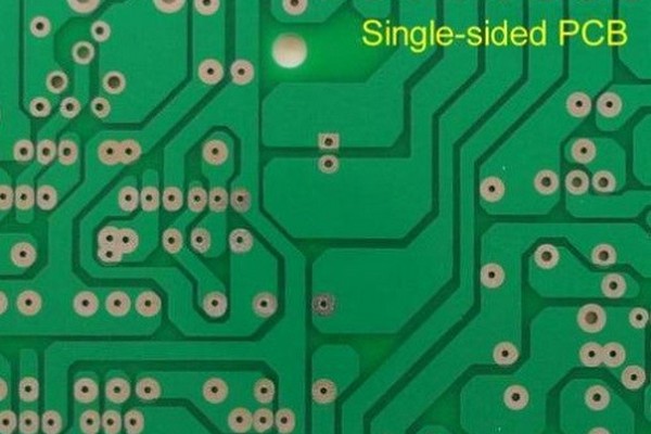
Single-sided printed circuit board can be considered as the simplest type of PCB produced. Because only one side of it consists of a conductive layer (usually copper). Single-sided printed circuit boards have almost the same performance as other PCBs and include an insulating layer called Core. The core can be made of different materials according to the properties of the final circuit, but the most common material used in this field is fiberglass. Normally, the production of the insulating core is done using a material known as 4FR.
Core is completely covered on one side with a thin layer of copper. In order to install parts on the board, holes are made on it. In the next step, copper will be removed during a process until the desired pads and paths are achieved for the electrical connection of the circuit components to each other. The upper part of the board is referred to as the side part, because the installation of the parts is done on this side, in such a way that we see their bases sticking out towards the bottom of the board, a place that is intended for easy soldering of the parts on the board. has been taken In the following, we will introduce double-sided PCB coating.
Double sided PCB printed circuit board
In terms of the final cover of the PCB iran, we must say that double-sided PCBs are a little more complicated compared to single-sided printed circuit boards, and in fact, copper is used on both the top and bottom sides of the core. This will provide more complex routing. According to the contract, the installation of perforated components in one-sided PCB layers is done on the top and surface mounting components are done on the bottom layer.
Printed circuit board drilling
Typically, double-sided boards will rely on through-hole components to create a connection between the bottom and top layers. Of course, this is not always possible, therefore, for double-sided PCBs, Plate Through Holes (PTH) are used as a common addition.

How to create a hole in a double-sided printed circuit board For double-sided PCB drilling, an electrolysis process is used to deposit copper inside the hole. This process will create a conductive path between the copper in the lower and upper layers.
Identifying types of final coating of printed circuit board
Soldering of most printed circuit board sets is done with the help of reflow method or wave soldering. As the name of the solder suggests, it is a repellent that will prevent the solder from sticking to the copper in parts of the board. Another advantage of soldering that can be mentioned is that the soldering process prevents copper corrosion on the PCB surface.
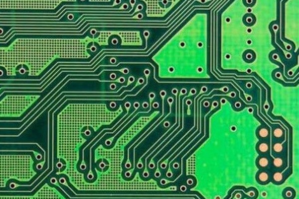
Until now, we have seen the description of printed circuits with one or two layers of copper. However, it is also possible to create PCBs that consist of more layers. These types of printed circuit boards are referred to as multilayer PCBs and are capable of providing better electrical noise characteristics and much denser routing topologies. In a multi-layer PCB, each layer is either a signal or a screen layer. Signal layers are used to transfer electrical signals from one component to another.
It is possible to produce multi-layer printed circuit boards in two ways, but the simplest type consists of thin double-sided PCB layers. The word Pre impregnated, which is an abbreviation of Prepreg, is a flexible material that is placed between rigid layers during construction, heated until the final processing is done well, and then it becomes hard. and helps to connect the layers and form the final structure. Determining the ratio of double-sided PCBs to prepreg layers is based on weight, cost and electromechanical issues.
 Confirm can be considered a thin film of protective material that is placed on the circuit board. If needed, it is able to cover the entire board and protects the board and its parts such as soldering connections, component covers and other metal parts. This will prevent metal corrosion and in addition, it will protect the entire screen from moisture, dust, spray, fungus and other contamination. This cover is even able to prevent damage caused by mechanical and thermal pressure.
Follow the articles of Arya Madar Arjomand and we hope to answer all your questions regarding the types of printed circuit boards and their coverage. I remind you that you can always call the phone numbers listed on the website and communicate with us directly.