printed circuit board
What is a printed circuit board (PCB) ?
The printed circuit board in iran( tehran) (PCB) is one of the intermediary electrical parts that plays a key role in the proper functioning of electronic equipment. Well, look inside any modern electronic device (TV, computer, mobile phone, washing machine, iron, kettle, etc.) and you will see one or more printed circuit boards, often referred to by the abbreviation PCB.
This piece consists of a single or multi-layer plate, which often includes a thin bottom board with a diameter of about 1.6 mm, which is made of materials such as fiberglass and resin. The other layer, which is still thin, will be made of copper to be conductive. If the copper layer is used only on one surface, it is called a single-sided printed circuit board (pcb iran) and if copper is on both sides, it is known as a double-sided printed circuit board. Copper is printed on the board and the required components of each circuit are soldered on it. In fact, this is the reason for the name of this piece. Printed circuits can be very complex or simple. In the picture, you can see a modern printed circuit board. A printed circuit board can accommodate tens or even hundreds of parts and establish communication between them..
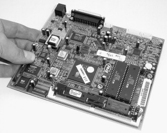
Printed circuit board
It may be said that the term "printing" is not a correct term for printed circuit boards (pcb tehran) because in fact the entire surface of the board is covered with copper and its insulating layers are included; Then the places where copper is needed, the insulation layer is removed and copper is applied and it will be completed based on the desired patterns of the design. Removing the layer is often done using very strong chemicals, so it is possible to use the conductivity of copper or create holes in the desired paths. The holes are used to pass the wire or in other words the communication between the layers. In the picture, you can see the cross-section of a printed circuit board, the places where the hole was created and the conductive surface was accessed.
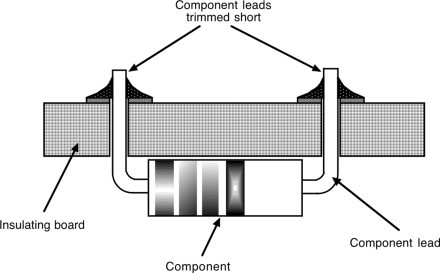
Printed circuit design
Printed boards (pcb iran or tehran) are the most common method of assembling modern electronic circuits. As mentioned above, boards consist of a sandwich of one or more insulation layers and one or more copper layers that contain components and voltage. Designing a modern printed circuit board is not an easy task and can be as tedious as designing a complete electrical circuit. Most of the modern systems of circuit boards consist of multi-layer boards, which in some cases may reach up to 32 layers. In traditional printed circuit boards, the components on the top layer were installed inside holes and were very primitive. Recently, with the advancement of technology, it is possible to design and implement the most complex printed circuit boards without the intervention of human hands and using modern devices; Just what you did inArya Madar ArajmandIt is done to print boards.
PCB design has a direct impact on the overall performance of the final system and must be designed and produced separately based on the needs of each device, which is considered a difficult task. The quality of used parts and the expertise of design engineers are very important in producing a board. Printed circuits should not have any energy leakage or voltage drop and show high resistance to humidity in the air or heat.
The printed circuit board can be divided into two general categories in terms of effect: boards that have the greatest impact on static or DC circuit performance and those that have the greatest impact on dynamic or AC circuit performance (especially at high frequencies). In any case, quality is important in every part of the design and production of the printed circuit board and is effective in the final performance of the part. Undoubtedly, the wrong paths and the use of low-quality material will cause you problems such as voltage reduction, outages, and lack of signal reception.
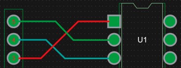
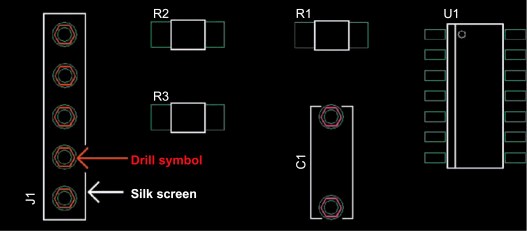
Designing a printed circuit board with a computer
There are many programs and devices for designing a printed circuit board, and in the past with one of them "Altium Designer or Protel" We met. The most important point in using the software is their accuracy and you must make sure that what you see on the screen is in accordance with the reality. The complete information of the layers, the exact items of the circuit board request, the location of the holes, the route of the coppers, the solder points and so on. The correct analysis of the assembly information must be perfect. In the programs, black color is often used for the background, so that you can recognize the effect of everything more accurately, and it is possible to correctly display each step separately and distinctly throughout the entire production process. You can see an example in the images. Look at the icons used to represent the hole locations and as you can see each color has a specific definition and each thing has its own ID.
Making PCB printed circuit board
The printed circuit board is made in different ways and in different stages based on the type and equipment; But in a standard way, the manufacturing steps are: raw PWBs, design, assembly of printed circuit boards, assembly of the system (if needed).
PWB test and measurement
This step includes checking continuity, checking short connections between wires, checking impedance and checking interference between signal conductors. Continuity indicates whether a signal can be transmitted from the source to the required destination. Here, the supervising engineer and system tester can check the short circuit between the wires if there is any problem. Impedance (the amount of opposition to alternating current) tests and helps check the integrity of other components.
PWB testing requires a device that allows checking different points on the PWB. The tester holds the board securely, provides the proper power, and allows the probe to sample signals from the test points on the PWB. This performance test is done with standard and high-quality devices and is very easy.
In other words, during testing, a technician or testing device stimulates points in a network circuit, records the results, and compares them with expected responses. Circuits that are well tested and fully scanned before production will work properly. The types of performance tests are a subset of all the tests performed on the circuit to approach the desired performance. An example of a functional test might be as simple as inputting a set of stimuli through buttons built into the system. It is important to use a method for testing to have the highest productivity in the manufacture and production of
printed circuit boards.
Computer trace board
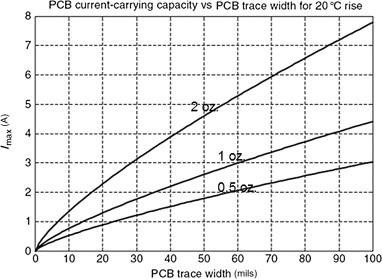
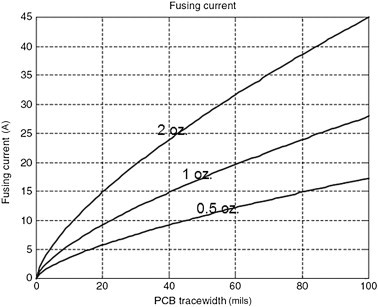
In the design and manufacture of printed circuit boards iran, it should be noted that the part is produced in the right size, and the size includes the width, thickness, and weight of the copper used in it, and it should be ensured that the current is transferred well without increasing the temperature. Resize or move. A rule of thumb says that a standard board that is 10mm wide and 1oz of copper can handle well over 500mA at 20 degrees above ambient. Copper weight versus thickness is shown in the table; You can also see the estimate of the current tolerance for a temperature increase of 20 degrees Celsius in the second table. As you can see the fusing current (diagram on the left) is significantly higher for the PC board.
| Miss weight |
Copper thickness (mm) |
| 0.5 |
0.7 mils |
| 1.0 |
1.4 mils |
| 2.0 |
2.8 mils |
Design steps of printed circuit board or PCB
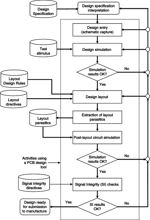
Overview: PCB design begins with an insulated base, and metal parts (electrical connections) and appropriate electronic components defined by the applicant are attached to this base. The key steps in the development of a PCB tehran are shown in the image below and we draw your attention to it:
You can use the online order button on the website to order the printed circuit board according to your needs with the right price and quality from Arjamand Arjamand company.
Start ordering printed circuit board
• At first, the designer's specification (document) is written, which actually defines the final performance required of the PCB. The information is transferred to the design programs and from there, the designer creates a circuit diagram that is entered into the PCB design tools.
• The overall design is completed and tested through modeling, then the performance of the design is verified. If the design does not meet the required specifications, either the design must be modified or, in cases where there are fundamental defects, the design specifications must be changed.
• Once the general design is complete, the PCB design is created taking into account the layout guidelines (approved by the respected Aria Madar company and in accordance with global standards) and the design rules of the manufacturing process.
• After the successful completion of the project, it is analyzed. The overall design is simulated (retested using specially designed tools to verify that the design works correctly). If there are any design problems or specifications, they need to be corrected.
• When all the planning stages are completed, the design is ready to be presented to the production department.
Metallized board and normal double-layer board
One of the terms that need to be familiar with is metallized board. Double-layer printed circuit boards, which are metallized, have pores and holes and are responsible for creating a connection between the layers. The two-layer boards have plated holes so that the communication between the layers can be done in the best way. In the so-called two-layer printed circuit boards, the holes located at the first and last of each crack are called PAD or VIA. Holes that have a separate part are pads, and if they are without additional assembly parts, they are holes. It should be noted that in metallized boards that have two layers, the connection between the layers is established by plating, and the difference between metallized and non-metallized and ordinary boards is also in this case, because ordinary boards do not have plating holes, and in this way, the connection between the layers is established. they do not. So it can be said that in normal circuit boards, we have two electrically separate layers.
Via types in multi-layer boards
It is worth noting that there are several types of wires in boards that have more than four layers, the most important of which are blind wires and wire wires. The blind via is connected to the upper or lower layer from one side and actually does not reach the other side and leads to the middle layer. The BURIED cut is connected between two surface layers and is placed inside the middle layer, so it is not visible from the outside. It is good to mention that the holes that communicate between two layers from one side of the circuit to the other are called holes or THROUGH HOLE.
Important points in the production and ordering of printed circuit boards
It can be said that almost every printed circuit (iran, tehran) has a different and special application and this is also true in similar products and it can be different. For example, the quality and type of printed circuits used in different products is one of the factors that when you buy an electronic device, you see that the speed, accuracy of performance or other things related to them are different in different brands. In other words, the PCB has a unique level of EMC performance, so how can we be sure that the existing printed circuit board has the performance we need?
It is recommended to use standard designs and not to confuse the designers with various ideas, but we at Aria Madar Arjmand have the ability to produce a wide range of types of printed circuits due to the opening of a new factory and professional staff, but we must always follow EMC standards. This standard specifies the conditions, methods and rules of electronic components.
The fact is that different designs can be considered for a PCB manufacturing order, but it should not be forgotten that using an incorrect design can increase your costs significantly. There is no fixed price for printed circuit boards and boards, and in order to estimate the order price of each circuit board, you must register your order in the order registration section, and our colleagues will determine the price of the part you want as soon as possible. Many factors are involved in the final price of the printed circuit board, and you should order the desired circuit from a company that you know produces the circuit with the highest quality, the most optimal cost, and using the most up-to-date devices. Accuracy in ordering and work experience are two of the most important factors influencing the purchase of the best type of circuit.
PCB recycling
So far, we have stated that the printed circuit board consists of a non-conductive base, a conductive layer (copper, aluminum, nickel, chrome and other metals) and the necessary electronic components and connections that are used in many devices that we use on a daily basis. They are used from electronic devices that are produced with the purpose of entertainment to devices such as mobile phones that are intertwined with everyone's life in the modern world. So, PCBs are considered an essential part and are produced on a large scale, and on the other hand, they are removed from production, and you cannot ignore their existence and do not think about recycling them. In the following two images, you can see a metal piece and the steps to make it.
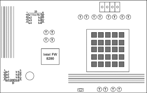

The statistics of 2006 indicate that 1 trillion dollars are earned from the sale of printed circuit boards per year, and among them personal computers were one of the most common devices in which printed circuit boards were used. You can see the main items used in a standard printed circuit board used for computers in the image below.
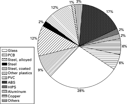
To recycle such a piece, it should be divided into several categories based on the ingredients:
The first part includes copper, aluminum, high-impact polystyrene (HIPS), acrylonitrile-butadiene-styrene (ABS), poly(vinyl chloride) and other functional plastics that are easier to recycle.
The second part includes all the steel and glass that can be recycled with simpler operations and includes 54%.
The last part is 15% and includes materials that are difficult to recycle.
Valuable materials inside the printed circuit
PCBs usually contain epoxy resin, fiberglass, copper, nickel, iron, aluminum and a certain amount of precious metals such as gold and silver. These materials and metals along with electronic components are connected to the screen by solder containing lead and tin. So far, the main composition of PCB materials has been determined. Sometimes the value of the metals used in these parts is higher than natural ore, but it should be noted that the recycling of these parts is very important for the environment. In the table below, you can see the average value of the items used in printed circuit boards with their prices. .
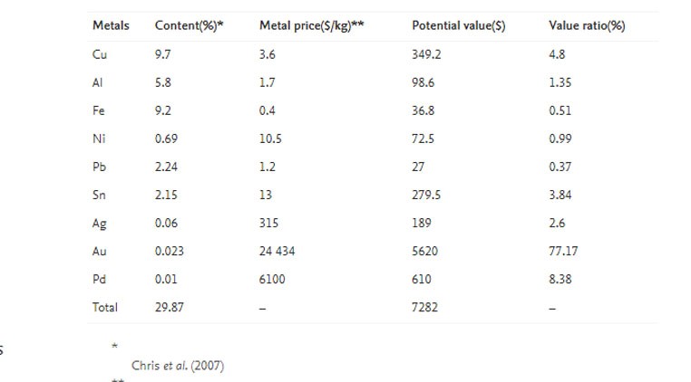
By studying the table, it can be seen that Au, Cu, Pd and Ag constitute almost all the material and economic value of waste printed circuit boards; Therefore, PCB recyclers are more focused on recovering these metals.
Printed circuit manufacturing industry in the world
Despite the complex technology and engineering required to produce printed circuit boards, we see that the United States, England, Germany and France still produce boards that have a competitive advantage; But the reality is that Asia produces three-quarters of the world's printed circuit boards, and more than 1,000 manufacturers are active in China alone. The PCB industry as a part of the electronics industry has always had its place in the world. However, in 2003, the United States produced 15% of the world's printed circuit boards, after Japan, the largest producer with 29%, China the second largest producer with 17%, and Taiwan the fourth largest producer in the world with 13%. Was. Europe accounted for only 10% and South Korea for 8%. No US company is currently in the top ten PCB manufacturers. China has overtaken Japan as the leader in PCB production.
Types of printed circuits
| SERIAL |
ITEM |
TECHNICAL DATA |
| 1 |
Board Type |
Rigid Board, RF |
| 2 |
Material |
FR4 Standard TG155 °C, ROGERS,
TEFLON
|
| 3 |
Layers |
1-8 Layers Pcb Prototype
|
| 4 |
Max Board Size |
400mm * 600mm |
| 5 |
Board Thickness |
0.25mm - 3.20mm |
| 6 |
Min line Width |
0.15 mm |
| 7 |
Min Space Width |
0.1 mm |
| 8 |
Min Hole Size |
0.2 mm |
| 9 |
Min Annular Ring |
0.15mm |
| 10 |
Copper Thickness |
35um - 70um |
| 11 |
Inner Layer Copper Thickness |
18um,35um |
| 12 |
Solder Mask Color |
Green, Black, White, Blue, Red, Yellow |
| 13 |
Silkscreen (Legend) Color |
White, Black, Yellow |
| 14 |
Surface Finishing |
HASL - Hot Air Solder Leveling
ENIG - Electro less Nickel / Immersion
Gold
|
| 15 |
Electrical Test |
Yes |
| 16 |
AOI (Automatic Optical Inspection) Test
|
Yes
|
| 17 |
Min Core Thickness For Multilayer
|
0.25 mm |
| 18 |
FR4 TG 140 °C Prepreg Specification For Multi layer
|
106 RC 71.5% 57um
1080 RC 62% 76um
2113 RC 56% 100um
2116 RC 53% 130um
7628 RC 43% 200um
|
Download the list of printed circuit types
PCB assembly prototype
If you intend to order a
printed circuit board in iran or tehran from Arjamand Aria Madar for the first time and you are not sure about the quality and service, we can prepare a prototype for you; It is enough to register a printed circuit board with desired features in the circuit order section so that we can price and produce that sample quickly. You can even order a lower quality prototype to make it affordable and cheaper to familiarize yourself with our process and quality. Be sure that we will provide you with the printed circuit you want through the best process available in the Iranian market and after the comprehensive tests we perform on it to ensure its accurate performance. This approach allows you to save money and spend less time searching for the right company to place your order.
Advantages of PCB Prototype Assembly
The reason for ordering a PCB prototype is that you can quickly assess how well your PCB design works. You cannot do this without going through the assembly process and be sure of our services. Fortunately, the venerable Aria circuit has the ability to assemble the PCB prototype in the best possible way, if you don't want to order a lot of printed circuit boards right away, so you can quickly see how well your assembled PCB prototype works.
While prototype assembly is typically produced in limited quantities, we bring the same high level of quality and precision to this process as we do on our full production assembly projects. We use the same resources and personnel to ensure the best possible results. Our capable team is fully qualified to handle every aspect of the process, including component procurement, circuit board fabrication, assembly fabrication and quality control. We will also follow your original design and produce the product exactly as you want. We will not make any changes without your approval and you can complete the entire process online from this website and order registration section.